成为一个前沿创新、高精度、全周期专业的半导体晶圆材料加工与技术服务供应商
To be a globally leading semiconductor wafer material processing and technology service provider
优质、定制、创新、发展
High quality、customized、innovative and advancement.

始终关注客户需求,为客户
企业和员工的共同发展而努力
Always pay attention to customer needs and strive for the common development of customers, enterprises, and employees

产品详情
details
产品详情

常规砷化铟_cover.jpg

常规砷化铟

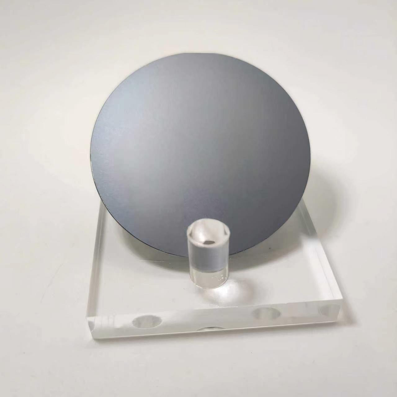
介绍:砷化铟InAs晶圆衬底电子迁移率高、磁阻效应低、 电阻温度系数小、窄带隙及优异光电等特性。

应用:适用于高频高速电子器件、红外探测、太赫兹技术和量子计算等领域。

产品规格书


砷化铟InAs单晶衬底(2~4inch)

直径

50.8mm

76.2mm

100mm

厚度

500μm

650μm

900μm

表面晶向

(100)0.1°off  toward(110)±0.05°

定位边长度

8±1mm

11±1mm

18±1mm

总厚度偏差TTV

<10μm

弯曲度Bow

<10μm

⠀⠀

掺杂元素

N/A

S-doping

S-doping

导电类型

N型

N型

N型

位错密度(EPD)/

2inch<1000;3inch<2500;4inch<4000;

载流子浓度

(1-3)E16/cm3

(4-8)E16/cm3

(1-3)E18/cm3

电子迁移率

>10000cm2/v.s

15000~25000cm2/v.s

7000-12000cm2/v.s


联系我们
contact us
0510-86886380
江苏省江阴市港城大道988号