⠀
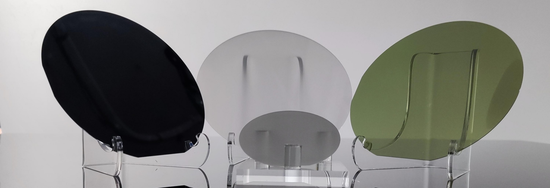
介绍:化学式(α-Al2O3),为六方晶格结构。化学性质非常稳定,不溶于水,耐强酸、强碱的腐蚀。莫氏硬度9级,熔点为2050℃,沸点3500℃,最高工作温度可达1900℃。透光性好,热传导性和电气绝缘性,力学机械性能表现优秀,具有耐磨和抗划伤的特点。
应用:PSS增强LED光提取效率,广泛应用于普通照明、背光源及显示领域;NPSS用于高端LED、激光器等精密光学和电子设备,进一步提升性能
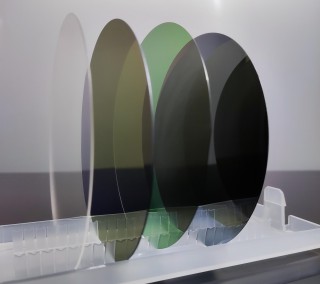
图形化PSS蓝宝石衬底晶片(2~6英寸)
直径
50.8mm
100mm
150mm
厚度
430μm
650μm
1000μm
表面晶向
C-plane(0001) off-angle toward M-axis(10-10) 0.2 +/- 0.1°
C-plane(0001) off-angle toward A-axis(11-20) 0 +/- 0.1°
定位边晶向
A-Plane(11-20) ± 1.0°
定位边长度
16mm
30mm
47.5mm
正面状态
Patterned
反面状态
SSP:Fine-ground,Ra=0.8-1.2um; DSP:Epi-polished,Ra<0.3nm
镭刻码面
Back side
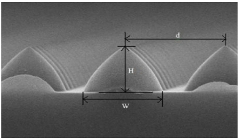
图形参数PSS
Shape Structure
Triangle Array
Pattern Height
1.6~1.8μm
Pattern Width
2.70~2.85μm
Pattern distance
2.9~3.1μm
图示PSS
纳米压印图形化NPSS蓝宝石衬底晶片(2~4英寸)
图形参数NPSS
Hexagonal Array
Pattern Type
V500
V600
V700
Pattern Diameter
400-550nm
550-650nm
650-750nm
250-450nm
Pattern Pitch
1000nm
V800
V900
∧700
750-850nm
850-950nm
600-800nm
350-550nm
350-700nm
图示NPSS


.png)